選擇合適的系列電壓基準(zhǔn)源的絕對(duì)精度電壓輸出

4.5V min
5.5V max
4.95V min
+12V available
4.75V min
5.25V max
VBATT)
2.7V min
3.6V max
*Reference voltage and DAC gain chosen for each design example
Design A: Low Cost, Loose Accuracy
For the Design-A example, VDD is 5V and the output range is 0-2.5V, so a 2.5V reference is used and the MAX5304 force/sense output is set to unity gain (OUT and FB pins shorted). A lower voltage reference could be used with a higher, externally set gain, but we have opted to save the two resistors for this low-cost design.Design B: High Absolute Accuracy and Precision
A 2.5V reference is chosen for the Design-B example, as the MAX5170 gain is fixed at 1.638 and a final output-voltage range of 0-4.096V is required. If a lower reference voltage is desired for Design B, a MAX5171 DAC could be used and its output force/sense gain could be set higher than 1.638 with external resistors, as shown in Figure 4. Note that the minimum VDD level is 4.95V, so the highest reference voltage we could use is 4.95V - 1.4V = 3.55V, as the DAC reference input is limited to (VDD - 1.4V)*.*This limit applies to all DACs mentioned in this article.
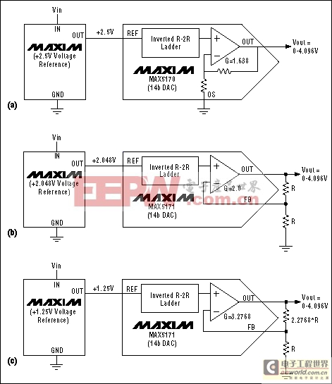
Figure 4. Design-B reference options: (a) 2.5V (chosen), (b) 2.048V, (c) 1.25V.
Design C: One-Time Calibrated, Low Drift
In the Design-C example, the MAX5154 has a fixed gain of 2, so a 2.048V reference provides a nominal 4.096V output at full-scale. This voltage must exceed our 4.000V design requirement, so that we can use a gain calibration to scale the voltage down to the 0V to 4V range. This design also has other reference-voltage options if the MAX5156 force/sense DAC is used. Note that the reference-input upper-limit voltage is 4.75V - 1.4V = 3.35V.Design D: Low Voltage, Battery Powered, Moderate Accuracy
The minimum VDD is 2.7V in the Design-D example, so the largest reference voltage that could be used is 2.7V - 1.4V = 1.3V. For this example, a 1.25V reference satisfies the 0V to 2.048V output range, as the MAX5176 gain is 1.638. It's important that the worst-case reference voltage, including all error terms, remains below 1.3V, or the specification for the DAC reference input voltage will be exceeded.Approximate dropout voltages were calculated for each of the design examples (Table 2). All of these voltages are well above the 200mV (or lower) dropout voltages typical of Maxim's voltage references. Because the upper reference input voltage of most Maxim DACs is limited to VDD - 1.4V, dropout voltages can normally be ignored with these designs if the DAC and the voltage reference use the same positive supply rail. The dropout voltages are approximate, because they were calculated without any error terms such as initial accuracy, but these errors are small compared to typical dropout voltages and can be ignored.
Step 2: Initial Voltage-Reference Device-Selection Criteria
There are many factors to consider when selecting the optimum reference for each design. To make the procedure manageable, candidate devices will be identified based on the reference voltage determined above, an estimate of required initial accuracy, an approximated temperature coefficient, and the reference output current needed for the chosen DAC (Table 3). Other factors such as cost, quiescent current, packaging, and a quick glimpse at the remaining specifications will be used to select a specific initial device for each design. The remaining specifications will be analyzed in the following section (Step 3) to determine if the devices satisfy the overall accuracy requirements.Table 3. Initial Device-Selection Considerations
相關(guān)推薦技術(shù)專區(qū)
|


評(píng)論