選擇合適的系列電壓基準源的絕對精度電壓輸出

Output error is often specified as a one-sided value (in LSBs at the DAC resolution), but it actually implies a double-sided error (Figure 3). For example, a 12-bit DAC with a 4.096V output range has an ideal LSB step size of 4.096V/4096 = 1mV. If the specified output error in this case is 4LSBs at 12-bit resolution, this means the DAC output at any code could be ±4LSBs (or ±4mV) from the ideal value. We define accuracy in terms of how many actual bits we have at our disposal to reach a desired output voltage with at most 1LSB of error:
Accuracy = DAC Resolution - log2(Error)In our example, we effectively have 10 bits (12 - log2(4)) of accuracy, because we can only get to within 1LSB at 10-bit resolution (±4mV = ±4/4096 = ±1/1024) of any given ideal DAC output value.
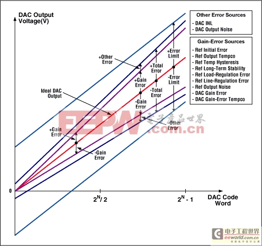
Figure 3. DAC transfer function and output error (zero offset assumed).
There are several sources that contribute to output error, but some (such as DAC offset) are ignored because they are not relevant to the reference-voltage selection process. Voltage-reference error sources that are considered include initial error, tempco, temperature hysteresis, long-term stability, load and line regulation, and output noise. DAC error sources include INL, gain error, gain-error tempco, and output noise.
Although the target error applies over the entire DAC code range, most of the error sources mentioned above cause an effective gain-error variation that is largest near the full-scale (highest DAC codes) of the transfer function (Figure 3). Gain errors are reduced with decreasing DAC code value; these errors are halved at midscale, and they virtually disappear near code zero, where offset error dominates. Error sources that do not exclusively affect the gain error and apply equally over most of the DAC code range include DAC INL and output noise.
INL is typically defined using one of two methods: absolute linearity or end-point linearity. Absolute linearity compares the DAC linearity to the ideal transfer-function linearity. End-point linearity uses the two measured end points to define the linearity (a straight line is drawn between these points), and all other points are compared to this line. In either case, INL should be included in the error analysis. In the latter case, the DAC INL error is zero at the end points, but can be present at DAC code words just inside these values. As an example, for a 12-bit DAC with INL defined between the end points of 0V and 4.095V (full-scale), the INL specification applies to DAC codes near 0 and 4095. For maximum error calculations, it is reasonable to add the DAC's INL and noise-induced output errors to the previously mentioned gain errors that are most severe near code 4095.
DAC Design Examples
To illustrate the steps involved with voltage-reference selection for DACs, a few design examples were created to cover a range of applications (Table 1). Only 10-, 12-, and 14-bit DAC designs are included in these examples, because they are the most instructive. The design steps are broken into individual sections by design examples (see Design A, Design B, and so forth).Table 1. Requirements for DAC Design Examples
Main Design Objectives | ||||
Example Application | ||||
DAC | ||||
Minimum Reference Input Resistance | ||||

相關推薦技術專區(qū) |


評論